 |
| |||||||||||||||||||||||||||||||||||||||||||||
Fri Sep 20 02:38:56 IST
Trains
| ♥♥All Imaginary Trains♥♥ | ||
| New Trains | To Be Introduced | |
| Special | Pending | |
| Festival | Special Fare | |
| Bedroll/Linen | LHB Rakes | |
| Vande Bharat | ||
| Namo Bharatnew | Amrit Bharat | |
| Humsafar | Antyodaya | |
| Tejas | Uday | |
| Rajdhani | Shatabdi | |
| Duronto | Garib Rath | |
| Sampark Kranti | Jan Shatabdi | |
| Suvidha | Premium Tatkal | |
| AC Express | AC SuperFast | |
| Mail/Express | SuperFast | |
| Passenger | Toy | |
| MEMU/DEMU | Double Decker | |
| Delhi EMU | Hyderabad | |
| Chennai EMU | Kolkata EMU | |
| Mumbai EMU | Pune EMU | |
ΣChains
| All ΣChains |
Atlas
| Main |
| Delhi Metro |
PNR
| Main |
| PNR #Follows |
| Recent Refreshes |
| Recent Refresh Requests |
| Blank PNRs |
| New PNRs |
| Recent Predictions |
| Recent Stampings |
| Surprises |
| Past Un-Stamped |
| Today's PNRs |
| Today's Un-Stamped |
| Tomorrow's PNRs |
| Tomorrow's Un-Stamped |
Forum
| Main | #Follows |
| Travel Tips | |
| Timeline | Travelogues |
| Polls | Popular |
| UnAnswered | Archived |
| Imaginary Train Blogs | Race Blogs |
Quiz
| Main Quiz Feed |
Gallery
| All Pics |
| All Station Pics |
| All Train Pics |
| All Loco Pics |
News
| Main |
| Major Accidents/Disruptions |
| New/Special Trains |
| Official Press Releases |
| Crime |
| Rail Budget |
| Trains in the News |
| Stations in the News |
Trips
| Trip Highlights |
| All Trips |
| Today's Departures |

#railwayengineering
******* Carbon emissions from Indian Railways in 2010 -2011 ********
It is a 9 Page PDF Document on Carbon emissions from...
more...
******* Carbon emissions from Indian Railways in 2010 -2011 ********
It is a 9 Page PDF Document on Carbon emissions from...
more...
Indian Railways during the Year 2010-2011.It is An estimation for transportation of goods during 2010-2011 which is prepared by :
Eswara Arun Kishore∗
Scientist-C
School of Maritime Design & Research
Indian Maritime University-Visakhapatnam: 530005
email: eakishore@gmail.com, arunkishoree@imu.co.in
The Main Summary of this Statistics are as Follows:
The following are the summary of the CO2 emissions evaluated for Indian railways freight movement during
2010-11:
1. CO2 emissions per Net-Tonne-km for diesel locomotive = 0.00951 grams.
2. CO2 emissions per Net-Tonne-km for electric locomotive = 0.01146 grams.
3. CO2 emissions per Net-Tonne-km for mixed goods train = 0.01072 grams.
• If the total goods were carried by diesel locomotives, the CO2 emissions would be =
2209.73/0.371 = 5956.15 Tonnes.
• If the total goods were carried by electric locomotives, the CO2 emissions would be =
4503.22/0.627 = 7182.17 Tonnes.
The PDF Document is attached with this BLOG for Ready Reference.
Download Link of the PDF Document :click here
Attached Image Link
click here
please wait...Translate to English
please wait...Translate to Hindi
Feb 12 2016 (17:28) CRJ/Chittaranjan (3 PFs) | GMO/WAG-9/31007 guest 6387 blog posts
Entry# 1737141 Tags Past Edits
Feb 12 2016 (6:09PM)
Loco Tag: GMO/WAG-9/31007 added by जीवन के सफ़र में राही मिलते हे बिछेर जानेको**/378817
Feb 12 2016 (6:09PM)
Station Tag: Chittaranjan/CRJ added by जीवन के सफ़र में राही मिलते हे बिछेर जानेको**/378817
Feb 12 2016 (6:08PM)
Station Tag: New Delhi/NDLS removed by जीवन के सफ़र में राही मिलते हे बिछेर जानेको**/378817
Feb 12 2016 (5:40PM)
Click on the "Summary" Tab to see the "Summary" View of total Suspected Bogies of WAG-9 in Indian Railway
(Screenshots of these Links are given below along with the Screenshot of the WAG-9 Monitoring Menu in E-Loco Website)
Feb 12 2016 (5:34PM)
Please Note that "VS" denotes the "Suspected Bogie of each WAG-9 which needs Proper Maintenance Attention" in the "Details" Format Sheet
Links Link are for Details Format is provided below:
(Screenshots of these Links are given below along with the Screenshot of the WAG-9 Monitoring Menu in E-Loco Website)
Feb 12 2016 (5:30PM)
Summary:
Click on the "Summary" Tab to see the "Summary" View
Loco Tag: GMO/WAG-9/31007 added by जीवन के सफ़र में राही मिलते हे बिछेर जानेको**/378817
Feb 12 2016 (6:09PM)
Station Tag: Chittaranjan/CRJ added by जीवन के सफ़र में राही मिलते हे बिछेर जानेको**/378817
Feb 12 2016 (6:08PM)
Station Tag: New Delhi/NDLS removed by जीवन के सफ़र में राही मिलते हे बिछेर जानेको**/378817
Feb 12 2016 (5:40PM)
Click on the "Summary" Tab to see the "Summary" View of total Suspected Bogies of WAG-9 in Indian Railway
(Screenshots of these Links are given below along with the Screenshot of the WAG-9 Monitoring Menu in E-Loco Website)
Feb 12 2016 (5:34PM)
Please Note that "VS" denotes the "Suspected Bogie of each WAG-9 which needs Proper Maintenance Attention" in the "Details" Format Sheet
(Screenshots of these Links are given below along with the Screenshot of the WAG-9 Monitoring Menu in E-Loco Website)
Feb 12 2016 (5:30PM)
Click on the "Summary" Tab to see the "Summary" View


#railwayengineering
********** Welcome Step taken by Indian Railways relating to Bogie Maintenance of WAG-9 Loco********
************ New Feature of E-Loco Website **********
We...
more...
********** Welcome Step taken by Indian Railways relating to Bogie Maintenance of WAG-9 Loco********
************ New Feature of E-Loco Website **********
We...
more...
all know that WAG-9 is a 3-Phase Freight Loco of IR and the Two Driver's Cabin(Front & Rear) of this Loco is known as Bogie 1 & Bogie 2. Here I am giving the WAG-9 List(Zone Wise) from E-Loco Website where you will see the "Suspected Bogie" of each WAG-9(Shown as "VS" in the List) which needs proper attention for maintenance. Please Note that "VS" denotes the "Suspected Bogie of each WAG-9 which needs Proper Maintenance Attention" in the "Details" Format Sheet. This List is in "Summary" Format & in "Details" Format. Link for Details Format is provided below:
Details: click here
Click on the "Summary" Tab to see the "Summary" View of total Suspected Bogies of WAG-9 in Indian Railway.
(Screenshots of these Links are given below along with the Screenshot of the WAG-9 Monitoring Menu in E-Loco Website)
Details: click here
Click on the "Summary" Tab to see the "Summary" View of total Suspected Bogies of WAG-9 in Indian Railway.
(Screenshots of these Links are given below along with the Screenshot of the WAG-9 Monitoring Menu in E-Loco Website)
please wait...Translate to English
please wait...Translate to Hindi
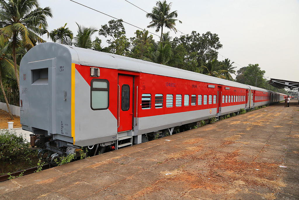
Feb 11 2016 (00:02) 12951/Mumbai Central - New Delhi Rajdhani Express | RCF/Kapurthala Rail Coach Factory (1 PFs) guest 6387 blog posts
Entry# 1735591 Tags Past Edits
Feb 11 2016 (12:47AM)
Train Tag: Mumbai Central - New Delhi Rajdhani Express/12951 added by KHUSIYA HO YA GAAM KABHI RUKE NA KADAM**/378817
Feb 11 2016 (12:30AM)
Image Link:
Feb 11 2016 (12:18AM)
Under Production the Programme above of Circumstance this can Unit we Exporting 2015-2016: Our LHB Coaches to Other Country ?
Under the above Circumstance can we Fancy for Exporting Our LHB Coaches to Other Country ?
Feb 11 2016 (12:15AM)
To Cross Checkthis these Figures you can refer this Link:
Under the above Circumstance can we Fancy for Exporting Our LHB Coaches to Other Country ?
Feb 11 2016 (12:05AM)
So, only 212 Coaches are made by this Unit(Which is the Main LHB Production Unit of IR) in every year on average in these past 11 years where the demand is huge for IR
Under the above Circumstance can we Fancy for Exporting Our LHB Coaches to Other Country ?
Feb 11 2016 (12:05AM)
Type of LHB Coaches mainly used in Indian Trains:
Under the above Circumstance can we Fancy for Exporting Our LHB Coaches to Other Country ?
Feb 11 2016 (12:03AM)
===== LHB COACH PRODUCTION REPORT OF RCF KAPURTHALA FROM: 01
========== FOR ZONE WISE DISTRIBUTION SUMMARY =============
Train Tag: Mumbai Central - New Delhi Rajdhani Express/12951 added by KHUSIYA HO YA GAAM KABHI RUKE NA KADAM**/378817
Feb 11 2016 (12:30AM)
Image Link:
Feb 11 2016 (12:18AM)
Under the above Circumstance can we Fancy for Exporting Our LHB Coaches to Other Country ?
Feb 11 2016 (12:15AM)
To Cross Check
Under the above Circumstance can we Fancy for Exporting Our LHB Coaches to Other Country ?
Feb 11 2016 (12:05AM)
So, only 212 Coaches are made by this Unit(Which is the Main LHB Production Unit of IR) in every year on average in these past 11 years where the demand is huge for IR
Under the above Circumstance can we Fancy for Exporting Our LHB Coaches to Other Country ?
Feb 11 2016 (12:05AM)
Type of LHB Coaches mainly used in Indian Trains:
Under the above Circumstance can we Fancy for Exporting Our LHB Coaches to Other Country ?
Feb 11 2016 (12:03AM)
===== LHB COACH PRODUCTION REPORT OF RCF KAPURTHALA FROM: 01
========== FOR ZONE WISE DISTRIBUTION SUMMARY =============
#railwayengineering
Ref: /news/post/256751 and /blog/post/1735117
===== LHB COACH PRODUCTION REPORT OF RCF KAPURTHALA FROM: 01.01.2005 TO 10.02.2016 ========
LS(Second class non self-generating): 153 Coaches
LGS(Second class self-generating): 66 Coaches
LWACCN[AC3...
more...
Ref: /news/post/256751 and /blog/post/1735117
===== LHB COACH PRODUCTION REPORT OF RCF KAPURTHALA FROM: 01.01.2005 TO 10.02.2016 ========
LS(Second class non self-generating): 153 Coaches
LGS(Second class self-generating): 66 Coaches
LWACCN[AC3...
more...
Air-conditioned 3-tier sleeping-car (72 berths)]: 623 Coaches
LWACCW[AC2 Air-conditioned 2-tier sleeping-car (52 berths)]: 266 Coaches
LWLRRM(Luggage/generator/brake van): 306 Coaches
LSCN(Second class 3-tier sleeper): 322 Coaches
LWCBAC(Air-conditioned pantry/kitchen/buffet car): 148Coaches
LWFAC[AC1 Air-conditioned first class sleeping-car (24 berths)]: 104Coaches
LWFCZAC[Air-conditioned executive chair car (56 seats)]: 30 Coaches
LWSCZAC[Air-conditioned chair car (78 seats)]: 209 Coaches
LWSCZ(Chair car): 106 Coaches
Total: 2333 Coaches in 11 years
Average: 212 Coaches per year
========== FOR ZONE WISE DISTRIBUTION SUMMARY =============
Please see the attached Word Document For Zone Wise Distribution Summary of each type of LHB Coaches in these 11 years
================================================== ==========================
To Cross Check these Figures you can refer this Link: click here
(Screenshot of this Link is attached)
Type of LHB Coaches mainly used in Indian Trains: click here
So, only 212 Coaches are made by this Unit(Which is the Main LHB Production Unit of IR) in every year on average in these past 11 years where the demand is huge for IR.
Production Programme of this Unit for 2015-2016: click here
Under the above Circumstance can we Fancy for Exporting Our LHB Coaches to Other Country ?
Image Link: click here
please wait...Translate to English
please wait...Translate to Hindi
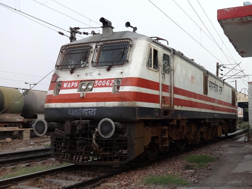
Feb 06 2016 (22:08) BRC/WAP-5/30062 guest 6387 blog posts
Entry# 1731833 Tags Past Edits
Feb 06 2016 (11:56PM)
Loco Tag: BRC/WAP-5/30062 added by JAI MAA TARA**/378817
Feb 06 2016 (10:35PM)
NB: As the available WAP-5 Coupling Videos are all of our IRI members
Hence shared this WAP-7 coupling Video
Feb 06 2016 (10:17PM)
Attached Image:
WAP5-BRC-30062 --- Spotted by Sam inside the NDLS loco trip shed while it was taking a nap on 12th July 2014
Link:
Courtesy: Sam

#railwayengineering
========== Crowned Gear Coupling Used in WAP-5 Locomotives ==========
What is Crowned Gear Coupling ?
Ans: Crowned gear coupling is meant for the connection between the motor and the gear transmission. This dual cardanic-acting...
more...
========== Crowned Gear Coupling Used in WAP-5 Locomotives ==========
What is Crowned Gear Coupling ?
Ans: Crowned gear coupling is meant for the connection between the motor and the gear transmission. This dual cardanic-acting...
more...
coupling transfers the torque from
the motor to the transmission and can compensate for radial, axial and angular shaft shifting. The inner toothed coupling sleeves are mounted rigidly on the
motor and transmission shaft. The coupling is equipped with separate, closed lubricant chambers in each coupling half. When removing or installing the motor or transmission, the lubricant chamber remains closed, eliminating the possibility of the toothing becoming dirty. The sealing elements are each arranged on the side facing the motor or transmission.
In this BLOG I have shared the 20 Page PDF Document approved by RDSO Lucknow on " REVISED SPECIFICATION FOR CROWNED GEAR COUPLING FOR WAP-5 AC ELECTRIC LOCOMOTIVES" Vide No: RDSO/2010/EL/SPEC/0107(REV ‘1’)
Download Link : click here
This PDF Document is attached with this BLOG for "Ready Reference".
Attached Video Details:
Video Title: 12301 Howrah Rajdhani being coupled with the most powerful locomotive in IR, WAP-7 of GZB Shed
Video Credits: Abhishek Chowdhury
Published on Nov 9, 2013
Video Description: This is the exclusive video of the Coupling of 12301 Howrah Rajdhani with the Most Powerful Locomotive in Indian Railways, WAP-7 of GZB Shed. This was at Howrah Terminus at 16:30 Hrs on 14th October,2013 (This year's Dashami) & was my first travel by Howrah Rajdhani. With the Maximum speed of 130 Km/h along with the Wi-Fi Facility makes this train not only the 5th fastest train but also technologically advanced train in the Indian Railways
Attached Image:
WAP5-BRC-30062 --- Spotted by Sam inside the NDLS loco trip shed while it was taking a nap on 12th July 2014.
Link: click here
Courtesy: Sam
NB: As the available WAP-5 Coupling Videos are all of our IRI members. Hence shared this WAP-7 coupling Video.
please wait...Translate to English
please wait...Translate to Hindi
Feb 04 2016 (23:23) CRJ/Chittaranjan (3 PFs) guest 6387 blog posts
Entry# 1729958 Tags Past Edits
Feb 05 2016 (12:29AM)
Ref:or
e WAP-5/WAP-7 & WAG-9] of Indian Railways)
Feb 05 2016 (12:29AM)
Ref: or([/blog/post/1513629/0)|[/blog/post/1513629/0)] |
e WAP-5/WAP-7 & WAG-9] of Indian Railways)
Feb 05 2016 (12:27AM)
********* Dedicated BLOG on Semiconductors and other relatedcomponenrs components used in the Semiconductors of 3-Phase Electric Locomotives in IR *****
Ref: or([/blog/post/1513629/0)| ([/blog/post/1513629/0)|[/blog/post/1513629/0)] |
e WAP-5/WAP-7 & WAG-9] of Indian Railways)
Feb 04 2016 (11:45PM)
********* Dedicated BLOG on Semiconductors and other relatedconcepts componenrs used in the Semiconductors of 3-Phase Electric Locomotives in IR *****
Ref: or( ([/blog/post/1513629/0)|
e WAP-5/WAP-7 & WAG-9] of Indian Railways)
Feb 04 2016 (11:41PM)
Ref: or (
e WAP-5/WAP-7 & WAG-9] of Indian Railways)
Feb 04 2016 (11:24PM)
In the above FAQ Post I describe all the details of GTO & IGBT Semiconductors and the difference between this Two
Ref:
e WAP-5/WAP-7 & WAG-9] of Indian Railways)
Feb 05 2016 (12:29AM)
Ref: or
e WAP-5/WAP-7 & WAG-9] of Indian Railways)
Feb 05 2016 (12:27AM)
********* Dedicated BLOG on Semiconductors and other related
Ref: or
e WAP-5/WAP-7 & WAG-9] of Indian Railways)
Feb 04 2016 (11:45PM)
********* Dedicated BLOG on Semiconductors and other related
Ref: or
e WAP-5/WAP-7 & WAG-9] of Indian Railways)
Feb 04 2016 (11:41PM)
Ref: or (
e WAP-5/WAP-7 & WAG-9] of Indian Railways)
Feb 04 2016 (11:24PM)
In the above FAQ Post I describe all the details of GTO & IGBT Semiconductors and the difference between this Two
#railwayengineering
********* Dedicated BLOG on Semiconductors and other related components used in the Semiconductors of 3-Phase Electric Locomotives in IR *****
Ref: /faq/post/1875
In the above FAQ Post I describe all the details of GTO & IGBT Semiconductors and the difference between this Two.
Ref:...
more...
********* Dedicated BLOG on Semiconductors and other related components used in the Semiconductors of 3-Phase Electric Locomotives in IR *****
Ref: /faq/post/1875
In the above FAQ Post I describe all the details of GTO & IGBT Semiconductors and the difference between this Two.
Ref:...
more...
/blog/post/1729028
In the above reply I describe the difference between a Thyristor(GTO i.e Gate Turn Off Thyristor) and Transistor(IGBT i.e Insulated Gated Bi-Polar Transistor)
Now in both of the above references one thing is Common that both GTO & IGBT are "SEMICONDUCTOR DEVICE" used in 3-Phase Locomotives. In perspective of this line it is now very Imperative to share the knowledge of "Semiconductor Device" in details here. So that all of you can know the Concept of "Semiconductor Device" in details.
Semiconductor Device:
Semiconductor devices are electronic components that exploit the electronic properties of semiconductor materials, principally silicon, germanium, and gallium arsenide, as well as organic semiconductors. Semiconductor devices have replaced thermionic devices (vacuum tubes) in most applications. They use electronic conduction in the solid state as opposed to the gaseous state or thermionic emission in a high vacuum.Semiconductor devices are manufactured both as single discrete devices and as integrated circuits (ICs), which consist of a number—from a few (as low as two) to billions—of devices manufactured and interconnected on a single semiconductor substrate, or wafer.Semiconductor materials are useful because their behavior can be easily manipulated by the addition of impurities, known as doping. Semiconductor conductivity can be controlled by introduction of an electric or magnetic field, by exposure to light or heat, or by mechanical deformation of a doped monocrystalline grid; thus, semiconductors can make excellent sensors. Current conduction in a semiconductor occurs via mobile or "free" electrons and holes, collectively known as charge carriers. Doping a semiconductor such as silicon with a small amount of impurity atoms, such as phosphorus or boron, greatly increases the number of free electrons or holes within the semiconductor. When a doped semiconductor contains excess holes it is called "p-type", and when it contains excess free electrons it is known as "n-type", where p (positive for holes) or n (negative for electrons) is the sign of the charge of the majority mobile charge carriers. The semiconductor material used in devices is doped under highly controlled conditions in a fabrication facility, or fab, to control precisely the location and concentration of p- and n-type dopants. The junctions which form where n-type and p-type semiconductors join together are called p–n junctions.
For more details and various Types of Semiconductor Device please refer: click here
What is p-nJunctions in c/w with Semiconductors?
Ans: A p–n junction is a boundary or interface between two types of semiconductor material, p-type and n-type, inside a single crystal of semiconductor. It is created by doping, for example by ion implantation, diffusion of dopants, or by epitaxy (growing a layer of crystal doped with one type of dopant on top of a layer of crystal doped with another type of dopant). If two separate pieces of material were used, this would introduce a grain boundary between the semiconductors that would severely inhibit its utility by scattering the electrons and holes.p–n junctions are elementary "building blocks" of most semiconductor electronic devices such as diodes, transistors, solar cells, LEDs, and integrated circuits; they are the active sites where the electronic action of the device takes place. For example, a common type of transistor, the bipolar junction transistor, consists of two p–n junctions in series, in the form n–p–n or p–n–p.The discovery of the p–n junction is usually attributed to American physicist Russell Ohl of Bell Laboratories.However, Vadim Lashkaryov reported discovery of p-n-junctions in Cu_2O and silver sulphide photocells and selenium rectifiers in 1941.A Schottky junction is a special case of a p–n junction, where metal serves the role of the p-type semiconductor.
For more details on p-njunction please refer: click here
What is p-type and n-type semiconductor material ?(Also known as Extrinsic Semiconductor)
Ans: click here
What is "Doping Agent/Dopant" used in Extrinsic Semiconductor ?
Ans: click here
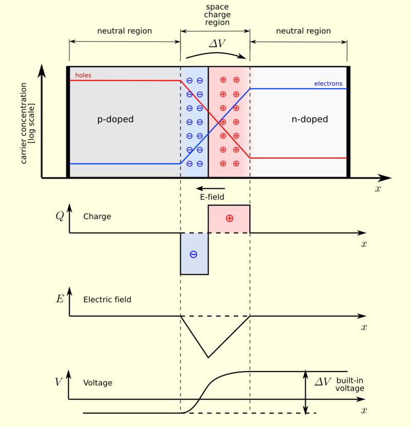
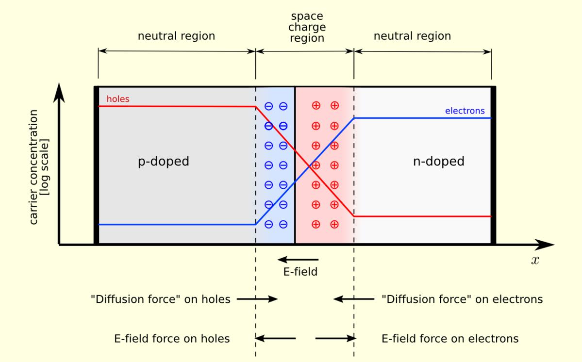
Attached Images:
An n–p–n bipolar junction transistor structure
Link: click here
Pn-junction-equilibrium
Link: click here
Pn-junction-equilibrium-graphs
Link: click here
(Hope from this BLOG all of you get a Complete Idea about Semiconductors used in 3-Phase Loco[i.e WAP-5/WAP-7 & WAG-9] of Indian Railways)
In the above reply I describe the difference between a Thyristor(GTO i.e Gate Turn Off Thyristor) and Transistor(IGBT i.e Insulated Gated Bi-Polar Transistor)
Now in both of the above references one thing is Common that both GTO & IGBT are "SEMICONDUCTOR DEVICE" used in 3-Phase Locomotives. In perspective of this line it is now very Imperative to share the knowledge of "Semiconductor Device" in details here. So that all of you can know the Concept of "Semiconductor Device" in details.
Semiconductor Device:
Semiconductor devices are electronic components that exploit the electronic properties of semiconductor materials, principally silicon, germanium, and gallium arsenide, as well as organic semiconductors. Semiconductor devices have replaced thermionic devices (vacuum tubes) in most applications. They use electronic conduction in the solid state as opposed to the gaseous state or thermionic emission in a high vacuum.Semiconductor devices are manufactured both as single discrete devices and as integrated circuits (ICs), which consist of a number—from a few (as low as two) to billions—of devices manufactured and interconnected on a single semiconductor substrate, or wafer.Semiconductor materials are useful because their behavior can be easily manipulated by the addition of impurities, known as doping. Semiconductor conductivity can be controlled by introduction of an electric or magnetic field, by exposure to light or heat, or by mechanical deformation of a doped monocrystalline grid; thus, semiconductors can make excellent sensors. Current conduction in a semiconductor occurs via mobile or "free" electrons and holes, collectively known as charge carriers. Doping a semiconductor such as silicon with a small amount of impurity atoms, such as phosphorus or boron, greatly increases the number of free electrons or holes within the semiconductor. When a doped semiconductor contains excess holes it is called "p-type", and when it contains excess free electrons it is known as "n-type", where p (positive for holes) or n (negative for electrons) is the sign of the charge of the majority mobile charge carriers. The semiconductor material used in devices is doped under highly controlled conditions in a fabrication facility, or fab, to control precisely the location and concentration of p- and n-type dopants. The junctions which form where n-type and p-type semiconductors join together are called p–n junctions.
For more details and various Types of Semiconductor Device please refer: click here
What is p-nJunctions in c/w with Semiconductors?
Ans: A p–n junction is a boundary or interface between two types of semiconductor material, p-type and n-type, inside a single crystal of semiconductor. It is created by doping, for example by ion implantation, diffusion of dopants, or by epitaxy (growing a layer of crystal doped with one type of dopant on top of a layer of crystal doped with another type of dopant). If two separate pieces of material were used, this would introduce a grain boundary between the semiconductors that would severely inhibit its utility by scattering the electrons and holes.p–n junctions are elementary "building blocks" of most semiconductor electronic devices such as diodes, transistors, solar cells, LEDs, and integrated circuits; they are the active sites where the electronic action of the device takes place. For example, a common type of transistor, the bipolar junction transistor, consists of two p–n junctions in series, in the form n–p–n or p–n–p.The discovery of the p–n junction is usually attributed to American physicist Russell Ohl of Bell Laboratories.However, Vadim Lashkaryov reported discovery of p-n-junctions in Cu_2O and silver sulphide photocells and selenium rectifiers in 1941.A Schottky junction is a special case of a p–n junction, where metal serves the role of the p-type semiconductor.
For more details on p-njunction please refer: click here
What is p-type and n-type semiconductor material ?(Also known as Extrinsic Semiconductor)
Ans: click here
What is "Doping Agent/Dopant" used in Extrinsic Semiconductor ?
Ans: click here
Attached Images:
An n–p–n bipolar junction transistor structure
Link: click here
Pn-junction-equilibrium
Link: click here
Pn-junction-equilibrium-graphs
Link: click here
(Hope from this BLOG all of you get a Complete Idea about Semiconductors used in 3-Phase Loco[i.e WAP-5/WAP-7 & WAG-9] of Indian Railways)
please wait...Translate to English
please wait...Translate to Hindi
Travel SAFE
1. RailFanning does NOT MEAN dangerous pics/videos.
2. Doorplating pics/youtube videos are strictly FORBIDDEN in IRI.
3. Take plenty of food pics and other safe pics.
4. Write human interest narratives to make the pics interesting.
5. Enjoy blogging and travelling SAFELY.
REMEMBER: YOUR LIFE is the most precious thing, NOT RailFanning.
Top Trending Posts
| 6173293 ★ 6 | AbhinavECR |
| 6194513 ★★ 22 | SSK |
| 6194172 ★ 8 | Siddharth98^~ |
| 4289126 ★ 8 | Siddharth98^~ |
| 4900117 ★★ 15 | Siddharth98^~ |
| 6188928 ★★ 13 | RailwayWithAniket |
| 6194722 ★★★ 44 | MLDTWAG9HC~ |
| 6177439 ★ 6 | arishabh1819~ |
| 6180206 ★★ 12 | BGKTWap7 |
| 6185874 ★★★ 27 | Nawaaz^~ |
| 6191326 ★ 10 | Exynos9611~ |
| 6192388 ★ 9 | PankajMishra^~ |
| 6193134 ★ 10 | Exynos9611~ |
| 6188926 ★ 8 | kirk781^~ |
| 6191448 ★★ 18 | PS9C~ |
| 6194867 ★ 9 | MSD~ |
| 6191869 ★★★ 74 | RahulKumarSharma~ |
| 6194658 ★★ 13 | kjmwag9hc^~ |
| 6193248 ★ 6 | RahulKumarSharma~ |
| 6193819 ★★ 21 | S_Bannerjee~ |
| 6194984 ★ 6 | BGKTWap7 |
| 6194716 ★★ 19 | PrakharYadav^~ |
| 6193603 ★★ 16 | Siddharth98^~ |
| 6194982 ★ 7 | Track_diaries^~ |
| 6194866 ★ 10 | ForeverRailfan^~ |
| 6184645 ★★ 13 | RohitBiharSharif~ |
| 6193299 ★ 11 | BGKTWap7 |
| 6192334 ★ 10 | BGKTWap7 |
| 6188307 ★ 8 | BGKTWap7 |
| 6194243 ★ 7 | BGKTWap7 |
Rail News
- झारखंड में रेलवे पटरी पर गिरी चट्टान, वंदे भारत समेत कई ट्रेनों के रूट में किया गया बदलाव
News Entry# 570237
by: Harshvardhan Gurjar Today (00:26)
झारखंड में रेलवे पटरी पर गिरी चट्टान, वंदे भारत समेत कई ट्रेनों के रूट में किया गया बदलाव click here - अब 'नमो भारत रैपिड रेल' नाम से जानी जाएगी भुज-अहमदाबाद वंदे मेट्रो, उद्घाटन से पहले बदला गया नाम
News Entry# 570236
by: Harshvardhan Gurjar Today (00:24)
Vande Bharat Metro: अब 'नमो भारत रैपिड रेल' नाम से जानी जाएगी भुज-अहमदाबाद वंदे मेट्रो, उद्घाटन से पहले बदला गया नाम click here - चिरेका में स्वच्छता ही सेवा के तहत वॉकथॉन का आयोजन
News Entry# 570235
by: Adittyaa Sharma Today (00:12)
चिरेका में गुरुवार को स्वच्छता ही सेवा अभियान के तहत वॉकथॉन का आयोजन किया गया.
मिहिजाम. चिरेगा में गुरुवार को स्वच्छता ही... - नवरात्रि के दौरान विंध्याचल स्टेशन पर होगा इन ट्रेनों का ठहराव, यहां देखें ट्रेनों की पूरी लिस्ट
News Entry# 570234
by: Harshvardhan Gurjar Today (00:11)
भारतीय रेलवे ने नवरात्रि के त्योहार को देखते हुए दिल्ली हावड़ा रेल रूट पर स्थित विंध्याचल स्टेशन पर कई ट्रेनों के स्टॉपेज दिए जाने की घोषणा की है, जिस... click here - ट्रेन के AC कोच में बेटिकट महिला यात्री ने किया हंगामा, टीटीई और RPF को दिखाया रौब
News Entry# 570233
by: Harshvardhan Gurjar Today (00:06)
बिहार के कटिहार में ट्रेन में बिना टिकट यात्रा के दौरान बर्थ पर बैठी महिला यात्री ने AC कोच में घंटों ड्रामा किया. वह वहां मौजूद टीटी और पैसेंजर के साथ बहस करती रहीं. महिला अधिवक्ताओं वाले यूनिफार्म में थी और खुद को लीगल एडवाइजर बताते हुए कोर्ट में आकर फैसला...
New Trains
- Type: ExpSPN/Shahjahanpur Junction to PBE/Pilibhit Junction
Run Dates: Sep 21 to Dec 31
Runs: Daily
Dep: 14:40 Arr: 16:30
Updated: Yesterday (21:04) - Type: ExpPBE/Pilibhit Junction to SPN/Shahjahanpur Junction
Run Dates: Sep 21 to Dec 31
Runs: Daily
Dep: 12:10 Arr: 13:55
Updated: Yesterday (20:59) - Type: ExpRGD/Rajgir to KIUL/Kiul Junction
Run Dates: Sep 18 to Dec 31
Runs: Daily
Dep: 06:10 Arr: 10:15
Updated: Yesterday (19:52) - Type: ExpKIUL/Kiul Junction to RGD/Rajgir
Run Dates: Sep 18 to Dec 31
Runs: Daily
Dep: 17:00 Arr: 21:25
Updated: Yesterday (19:51) - Type: SFVSKP/Visakhapatnam Junction to SHM/Shalimar (Kolkata)
Run Date: ONLY ON Oct 01
Runs: Tue
Dep: 11:20 Arr: 03:00 +1
Updated: Yesterday (18:56) - Type: ExpARK/Araku to VSKP/Visakhapatnam Junction
Run Dates: Oct 05 to Oct 15
Runs: Daily
Dep: 14:00 Arr: 18:00
Updated: Yesterday (18:16) - Type: ExpVSKP/Visakhapatnam Junction to ARK/Araku
Run Dates: Oct 05 to Oct 15
Runs: Daily
Dep: 08:30 Arr: 11:30
Updated: Yesterday (18:09) - Type: SFDKBJ/Dahar Ka Balaji to PUNE/Pune Junction
Run Dates: Oct 31 to Nov 07
Runs: Thu
Dep: 10:30 Arr: 09:30 +1
Updated: Yesterday (22:04) - Type: ACSFPUNE/Pune Junction to MFP/Muzaffarpur Junction
Run Dates: Apr 29 to Oct 28
Runs: Mon
Dep: 06:30 Arr: 15:15 +1
Updated: Yesterday (14:02) - Type: ACSFMFP/Muzaffarpur Junction to PUNE/Pune Junction
Run Dates: Apr 27 to Oct 26
Runs: Sat
Dep: 21:15 Arr: 05:35 +2
Updated: Yesterday (14:01)
Site Announcements
- Entry# 5648027
Mar 01 2023 (12:44AM)
In response to past confusions with Train/Station updates and resulting fights and controversies, the following clear and objective guidelines are being issued, with no room for any arguments or debates about validity. Also, included, some other changes with respect to Ratings. 1. All Red Ratings will require further explanation. Red Ratings won't... - Entry# 5388512
Jun 24 2022 (08:45AM)
As announced previously, there are a few changes coming to IRI user accounts, based on past practices. 1. As before, you will be able to quickly DELETE your IRI User account at ANY time. However, the menu option for this was hidden in the profile page, and could not easily be located.... - Entry# 5148000
Nov 29 2021 (06:40AM)
A new feature will be released soon, whereby you can follow blogs tagged with specific Trains & Stations. If you have already posted blogs tagged with some Train/Station, then you will be set to automatically follow that Train/Station. Thereafter, any future news/blogs tagged with those Trains/Stations will be marked to your... - Entry# 5093784
Oct 13 2021 (07:04AM)
These days, every other day, we are getting requests from members to allow email login to their FB-based IRI account. 10 years ago, we had given the option for users to login through FaceBook - in retrospect, this was a mistake. These days, apparently, users are quitting FaceBook in droves because... - Entry# 4906979
Mar 14 2021 (01:12AM)
Followup to: Fmt Changes The new version of FmT 2.0 will soon be here - in about 2 weeks. As detailed in the previous announcement, many of the old FmT features like Train TT, Speedometer, Geo Location, etc. will be REMOVED. It will be a bare-bones simple app, focused on trip blogging. It... - Entry# 4898771
Mar 06 2021 (10:33PM)
There are some changes coming to FMT. Many of the features of FMT, like station arrival, TT, speed, geo, passing times, station time, etc. are ALREADY available in OTHER railway apps. So all of these features will be REMOVED. We'll have ONLY BLOGGING - quick upload of pics/videos/audio, etc. You may attach...
Member Blog Links
Scroll to Top